Cirrus-logic CS4202 User Manual
Browse online or download User Manual for Hardware Cirrus-logic CS4202. Cirrus Logic CS4202 User Manual
- Page / 66
- Table of contents
- BOOKMARKS
- Features 1
- Description 1
- TABLE OF CONTENTS 2
- LIST OF FIGURES 4
- LIST OF TABLES 5
- MIXER CHARACTERISTICS 7
- 9
- 10 DS549PP2 10
- Figure 1. Power Up Timing 10
- Figure 3. Clocks 10
- DS549PP2 11 11
- Figure 6. Test Mode 11
- 2. GENERAL DESCRIPTION 12
- 2.1 AC-Link 12
- 2.2 Control Registers 13
- 2.3 Sample Rate Converters 13
- 2.4 Mixers 13
- 2.5 Input Mux 13
- 2.6 Volume Control 13
- 14 DS549PP2 14
- 3. AC-LINK FRAME DEFINITION 15
- 20 DS549PP2 20
- 4. REGISTER INTERFACE 21
- 0000000ID8ID700ID40000 22
- Mute 0 ML5 22
- 00000SL2SL1SL000000SR2SR1SR0 26
- 000000MIXMSLPBK0000000 28
- 11111111111GP4GP3GP2GP1GP0 35
- 00000000000GS4GS3GS2GS1GS0 35
- 5. SERIAL DATA PORTS 42
- 5.1 Overview 42
- 5.2 Multi-Channel Expansion 42
- 5.3 Serial Data Formats 43
- 6. SONY/PHILIPS DIGITAL 44
- INTERFACE (S/PDIF) 44
- 7. EXCLUSIVE FUNCTIONS 44
- DS549PP2 45 45
- 8.2 Powerdown Controls 46
- + DVdd/Rload/2 47
- 9. CLOCKING 48
- 9.3 Secondary Codec Operation 48
- 22 pF 22 pF 49
- 24.576 MHz 49
- 50 DS549PP2 50
- Figure 19. Differential 1 V 50
- CD Input 50
- 10.1.4 PC Beep Input 51
- 10.1.5 Phone Input 51
- 10.2 Analog Outputs 51
- 10.2.1 Stereo Outputs 51
- 10.2.2 Mono Output 52
- 10.4 Power Supplies 52
- 10.5 Reference Design 53
- 11. GROUNDING AND LAYOUT 54
- DS549PP2 55 55
- CS4202 48-pin 56
- Package Layout 56
- Audio I/O Pins 57
- AC-Link Pins 59
- Clock and Configuration Pins 60
- Misc. Digital Interface Pins 60
- Power Supply Pins 61
- 14.REFERENCE DESIGN 64
- 15.REFERENCES 65
- 48L LQFP PACKAGE DRAWING 66
Summary of Contents
Preliminary Product InformationThis document contains information for a new product.Cirrus Logic reserves the right to modify this product without not
CS420210 DS549PP2BIT_CLKTrst_lowTrst2clkTvdd2rst#VddRESET#Figure 1. Power Up TimingFigure 2. Codec Ready from Start-up or Fault ConditionBIT_CLKTsyn
CS4202DS549PP2 11BIT_CLKTisetupTiholdTcoSDATA_OUT,SYNCSDATA_INFigure 4. Data Setup and HoldBIT_CLKTs2_pdownSDATA_INSDATA_OUTSYNCWrite to 0x20 Data PR
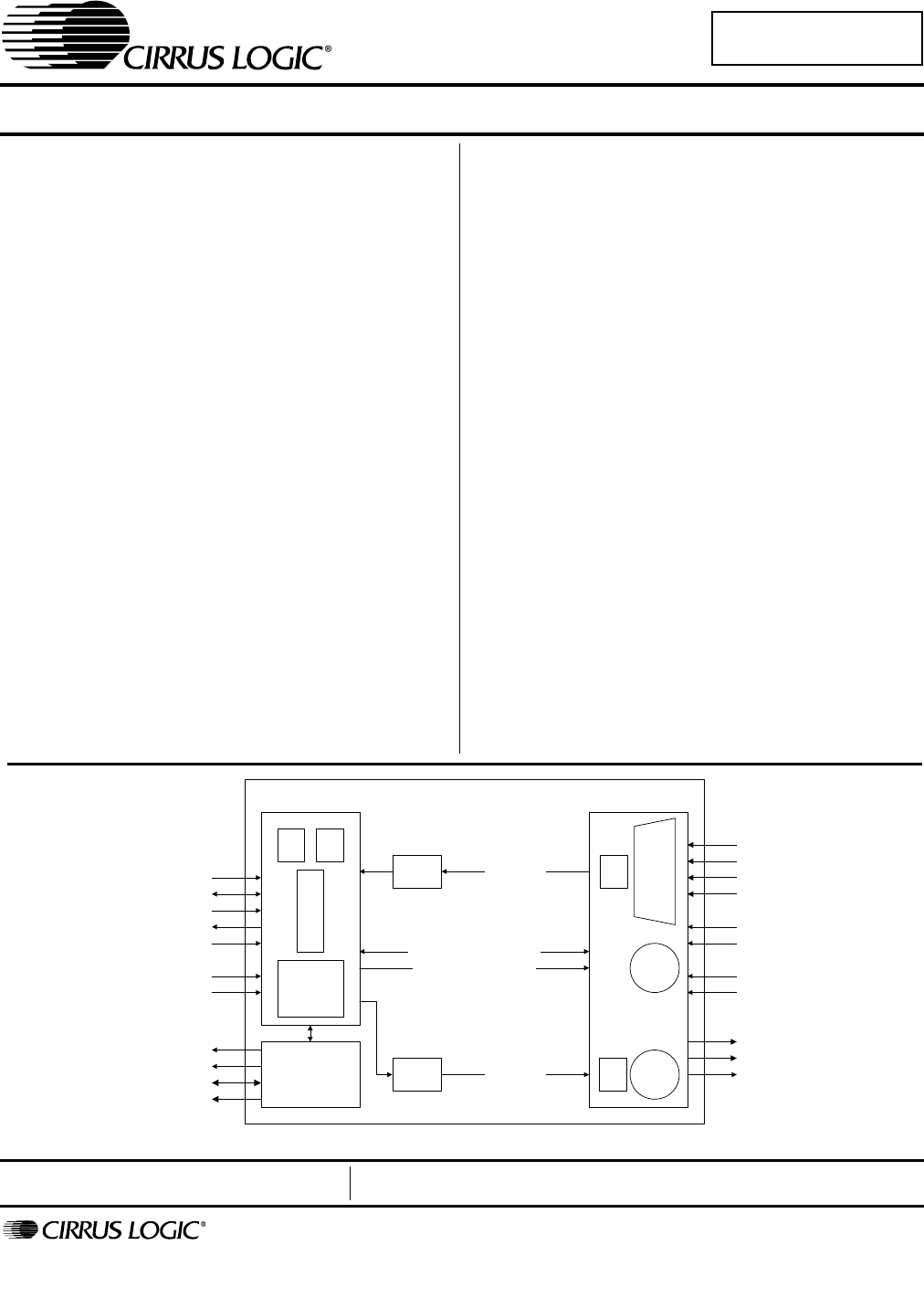
CS420212 DS549PP22. GENERAL DESCRIPTIONThe CS4202 is a mixed-signal serial audio codecwith integrated headphone power amplifier com-pliant with the In
CS4202DS549PP2 132.2 Control RegistersThe CS4202 contains a set of AC ’97 compliantcontrol registers, and a set of Cirrus Logic definedcontrol registe
CS420214 DS549PP2VOLMUTEVOLMUTEVOLMUTEVOL VOLMUTEVOL VOL VOLMUTEBOOSTΣΣ1/2OUTPUTBUFFERHEADPHONEAMPLIFIEROUTPUTBUFFERVOL VOLADCINPUTMUXVOLADCMUTEPCM_OU
CS4202DS549PP2 153. AC-LINK FRAME DEFINITIONThe AC-link is a bi-directional serial port with dataorganized into frames consisting of one 16-bit andtwe
CS420216 DS549PP23.1 AC-Link Serial Data Output FrameIn the serial data output frame, data is passed on the SDATA_OUT pin to the CS4202 from the AC ’9
CS4202DS549PP2 173.1.3 Command Data Port (Slot 2)WD[15:0] Write Data. The WD[15:0] bits contain the 16-bit value to be written to the register. If an
CS420218 DS549PP23.2 AC-Link Serial Data Input FrameIn the serial data input frame, data is passed on the SDATA_IN pin from the CS4202 to the AC ’97 c
CS4202DS549PP2 193.2.3 Status Data Port (Slot 2)RD[15:0] Read Data. The RD[15:0] bits contain the register data requested by the controller from the p
CS42022 DS549PP2 TABLE OF CONTENTS1. CHARACTERISTICS AND SPECIFICATIONS ... 7ANA
CS420220 DS549PP23.3 AC-Link Protocol Violation - Loss of SYNCThe CS4202 is designed to handle SYNC protocolviolations. The following are situations w
CS4202DS549PP2 214. REGISTER INTERFACE Reg Register Name D15 D14 D13 D12 D11 D10 D9 D8 D7 D6 D5 D4 D3 D2 D1 D0 Default00hReset 0 0 0 0 0 0 0 ID8 ID7
CS420222 DS549PP24.1 Reset Register (Index 00h) ID8 18-bit ADC Resolution. The ID8 bit is ‘set’, indicating this feature is present.ID7 20-bit DAC res
CS4202DS549PP2 234.3 Mono Volume Register (Index 06h)Mute Mono Mute. Setting this bit mutes the MONO_OUT output signal. MM[5:0] Mono Volume Control. T
CS420224 DS549PP24.6 Microphone Volume Register (Index 0Eh)Mute Microphone Mute. Setting this bit mutes the MIC1 or MIC2 signal. The selection of the
CS4202DS549PP2 254.7 Analog Mixer Input Gain Registers (Index 10h - 18h)Mute Stereo Input Mute. Setting this bit mutes the respective input signal, bo
CS420226 DS549PP24.8 Input Mux Select Register (Index 1Ah)SL[2:0] Left Channel Source. The SL[2:0] bits select the left channel source to pass to the
CS4202DS549PP2 274.9 Record Gain Register (Index 1Ch) Mute Record Gain Mute. Setting this bit mutes the input to the L/R ADCs.GL[3:0] Left ADC Gain. T
CS420228 DS549PP24.10 General Purpose Register (Index 20h) MIX Mono Output Path. This bit controls the source of the mono output driver. When ‘cle
CS4202DS549PP2 294.11 Powerdown Control/Status Register (Index 26h)EAPD External Amplifier Power Down. The EAPD pin follows this bit and is generally
CS4202DS549PP2 34.4 PC_BEEP Volume Register (Index 0Ah)... 244.5 Phone Volume R
CS420230 DS549PP24.12 Extended Audio ID Register (Index 28h)ID[1:0] Codec ID. These bits indicate the current codec configuration. When ID[1:0] = 00,
CS4202DS549PP2 314.13 Extended Audio Status/Control Register (Index 2Ah)SPCV S/PDIF Configuration Valid. This read-only bit indicates the status of th
CS420232 DS549PP24.14 Audio Sample Rate Control Registers (Index 2Ch - 32h) SR[15:0] Sample Rate Select. The Audio Sample Rate Control Registers (Inde
CS4202DS549PP2 334.15 S/PDIF Control Register (Index 3Ah)V Validity. The V bit is mapped to the V bit (bit 28) of every sub-frame. If this bit is ‘cle
CS420234 DS549PP24.16 Extended Modem ID Register (Index 3Ch) ID[1:0] Codec ID. These bits indicate the current codec configuration. When ID[1:0] = 00,
CS4202DS549PP2 354.19 GPIO Pin Polarity/Type Configuration Register (Index 4Eh) GP[4:0] GPIO Pin Configuration. This register defines the GPIO input p
CS420236 DS549PP24.21 GPIO Pin Wakeup Mask Register (Index 52h) GW[4:0] GPIO Pin Wakeup. This register provides a mask for determining if an input GPI
CS4202DS549PP2 37from the ADC output.TMM True Mono Mode. The TMM bit controls the source of the stereo-to-mono mixer that feeds into the mono out sele
CS420238 DS549PP24.24 Misc. Crystal Control Register (Index 60h)DPC DAC Phase Control. This bit controls the phase of the PCM stream sent to the DACs
CS4202DS549PP2 394.25 Serial Port Control Register (Index 6Ah)SDEN Serial Data Output Enable. The SDEN bit enables transmission of serial data on the
CS42024 DS549PP210.4 Power Supplies ... 531
CS420240 DS549PP24.26 BIOS-Driver Interface Control Registers (Index 70h - 72h)E[15:0] Event Configuration. The E[15:0] bits control the BIOS-Driver I
CS4202DS549PP2 414.28 Vendor ID1 Register (Index 7Ch)F[7:0] First Character of Vendor ID. With a value of F[7:0] = 43h, these bits define the ASCII ‘C
CS420242 DS549PP25. SERIAL DATA PORTS5.1 OverviewThe CS4202 implements two serial data outputports that can be used for multi-channel expansion.Each s
CS4202DS549PP2 435.3 Serial Data FormatsIn order to support a wide variety of serial audioDACs, the CS4202 can transmit serial data in fourdifferent f
CS420244 DS549PP26. SONY/PHILIPS DIGITAL INTERFACE (S/PDIF)The S/PDIF digital output is used to interface theCS4202 to consumer audio equipment extern
CS4202DS549PP2 458. POWER MANAGEMENT8.1 AC ’97 Reset ModesThe CS4202 supports four reset methods, as de-fined in the AC ’97 Specification: Cold Reset,
CS420246 DS549PP28.2 Powerdown ControlsThe Powerdown Control/Status Register(Index 26h) controls the power management func-tions. The PR[6:0] bits in
CS4202DS549PP2 47PR Bit ADCs DACs MixerAnalog ReferenceACLinkInternal Clock Off HeadphonePR0•PR1 •PR2 ••• •PR3 ••• • •PR4 •PR5 •• •PR6 •Table 16. Powe
CS420248 DS549PP29. CLOCKINGThe CS4202 may be operated as a primary or sec-ondary codec. As a primary codec, the system clockfor the AC-link may be ge
CS4202DS549PP2 4922 pF 22 pF24.576 MHzDGNDXTL_OUTXTL_INFigure 17. External Crystal External Clock on XTL_INID1# ID0#AC-Link Timing ModeCodec IDClock
CS4202DS549PP2 5LIST OF TABLESTable 1. Register Overview for the CS4202 ...22Table 2
CS420250 DS549PP210.ANALOG HARDWARE DESCRIPTIONThe analog input section consists of four stereoline-level inputs (LINE_L/R, CD_L/C/R,VIDEO_L/R, and AU
CS4202DS549PP2 51Mic Volume Register (Index 0Eh) the pre-amplifiergain can be set to 0 dB, 10 dB, 20 dB, or 30 dB. 10.1.4 PC Beep Input The PC_BEEP i
CS420252 DS549PP2the part behaves as specified in AC ’97. As shown inFigure 24, if the HPCFG pin is grounded, the part be-haves as if HP_OUT was the o
CS4202DS549PP2 53digital supply as the controller’s AC-link interface.Since the digital interface on the CS4202 may oper-ate at either +3.3 V or +5 V,
CS420254 DS549PP211. GROUNDING AND LAYOUTFigure 26 on page 55 shows the conceptual layoutfor the CS4202 in XTAL or OSC clocking modes.The decoupling c
CS4202DS549PP2 55 AnalogGroundPin 10.1 µF1000 pFNPO2.2µF0.1 µFY5V0.1 µFY5VY5V0.1 µFY5VAVdd2AVAFLT2REFFLTAVss1AVdd1AFLT1Via to +5VD or +3.3VDVia to +5V
CS420256 DS549PP212. PIN DESCRIPTIONS CS4202 48-pinPackage Layout36 35 34 33 32 31 30 29 28 27 26 251314151617181920212223241 2 3 4 5 6 7 8 9 10 11
CS4202DS549PP2 57Audio I/O PinsPC_BEEP - Analog Mono Source, Input, Pin 12The PC_BEEP input is intended to allow the PC system POST (Power On Self-Tes
CS420258 DS549PP2VIDEO_L, VIDEO_R - Analog Video Audio Source, Inputs, Pins 16 and 17These inputs form a stereo input pair to the CS4202. It is intend
CS4202DS549PP2 59AFLT1 - Left ADC Channel Antialiasing Filter, Input, Pin 29This pin needs a 1000 pF NPO capacitor connected to analog ground.AFLT2 -
CS42026 DS549PP21. CHARACTERISTICS AND SPECIFICATIONSANALOG CHARACTERISTICS (Standard test conditions unless otherwise noted: Tambient = 25° C, AVdd =
CS420260 DS549PP2Clock and Configuration PinsXTL_IN - Crystal Input / Clock Input, Pin 2This pin requires either a 24.576 MHz crystal, with the other
CS4202DS549PP2 61GPIO2 - General Purpose I/O, Input/Output, Pin 32This pin is a general purpose I/O pin that can be used to interface with various ext
CS420262 DS549PP213.PARAMETER AND TERM DEFINITIONSAC ’97 SpecificationRefers to the Audio Codec ’97 Component Specification Ver 2.2 published by the I
CS4202DS549PP2 63Interchannel IsolationThe amount of 1 kHz signal present on the output of the grounded AC-coupled line input channel with 1kHz, 0 dB,
CS420264 DS549PP214.REFERENCE DESIGN R186.8KC23 1uFY5VR14 6.8KC3122pFNPOC22 1uFY5VC3222pFNPOJ112R11 6.8KR4 220KJ443521C252.2uFY5VC310uFELEC+R9 47
CS4202DS549PP2 6515.REFERENCES1) Cirrus Logic, Audio Quality Measurement Specification, Version 1.0, 1997http://www.cirrus.com/products/papers/meas/me
CS420266 DS549PP216.PACKAGE DIMENSIONSINCHES MILLIMETERSDIM MIN NOM MAX MIN NOM MAXA --- 0.055 0.063 --- 1.40 1.60A1 0.002 0.004 0.006 0.05 0.10 0.15B
CS4202DS549PP2 7ANALOG CHARACTERISTICS (Continued) MIXER CHARACTERISTICS ABSOLUTE MAXIMUM RATINGS (AVss1 = AVss2 = DVss1 = DVss2 = 0 V)RECO
CS42028 DS549PP2DIGITAL CHARACTERISTICS (AVss1 = AVss2 = DVss1 = DVss2 = 0 V) Parameter Symbol Min Typ Max UnitDVdd = 3.3VLow level input voltage V
CS4202DS549PP2 9AC ’97 SERIAL PORT TIMING Standard test conditions unless otherwise noted: Tambient = 25° C, AVdd = 5.0 V, DVdd = 3.3 V; CL = 55 pF lo
Related products and manuals for Hardware Cirrus-logic CS4202
 (24 pages)
(18 pages)
(51 pages)
(81 pages)
(148 pages)
(22 pages)
(10 pages)
(6 pages)
(32 pages)
(34 pages)
(32 pages)
(79 pages)
(72 pages)
(72 pages)
(72 pages)
(16 pages)
(72 pages)
(4 pages)
(32 pages)
(63 pages)
(24 pages)
(18 pages)
(51 pages)
(81 pages)
(148 pages)
(22 pages)
(10 pages)
(6 pages)
(32 pages)
(34 pages)
(32 pages)
(79 pages)
(72 pages)
(72 pages)
(72 pages)
(16 pages)
(72 pages)
(4 pages)
(32 pages)
(63 pages)
© 2020, manymanuals.com. All rights reserved. | 2.435 s |
 Manymanuals.com
 Manymanuals.de
 Manymanuals.fr
 Manymanuals.it
 Manymanuals.pl
 Manymanuals.cz
 Manymanuals.es
 Manymanuals-pt.com
Comments to this Manuals