Cirrus-logic AN241 User Manual
Browse online or download User Manual for Hardware Cirrus-logic AN241. Cirrus Logic AN241 User Manual
- Page / 16
- Table of contents
- BOOKMARKS
Summary of Contents
1Copyright Cirrus Logic, Inc. 2003(All Rights Reserved)http://www.cirrus.comAN241Analog Input Buffer Architecturesby Kevin L Tretter1. IntroductionT
AN241104.6 Overview of Filter Topology #24.6.1 High Pass Filter and DC BiasingThe first stage of the buffer forms a high pass filter from the combinat
AN24111the converter is susceptible to aliasing). The characteristics of this low pass filter can be changed by ad-justing the values of the resistors
AN241124.8 Overview of Filter Topology #34.8.1 Op Amp CircuitryThe op-amp topology used in the input buffer shown in Figure 6 addresses two issues. Fi
AN241134.8.3 Anti-Aliasing CapacitorFigure 6 implements a common mode capacitor between the analog input and the associated referencevoltage pin on ea
AN24114Figure 7. Single Ended Input Buffer with a Common Reference Pin5.4 Overview of Filter Topology5.4.1 High Pass Filter and DC BiasingThe first s
AN24115In the input buffer shown in Figure 7, REQ ≈ 50 kΩ (100 kΩ RkΩ) and C = 4.7µF. This places the 3 dBcorner at approximately 0.68 Hz. Typically
AN24116.Contacting Cirrus Logic SupportFor a complete listing of Direct Sales, Distributor, and Sales Representative contacts, visit the Cirrus Logic
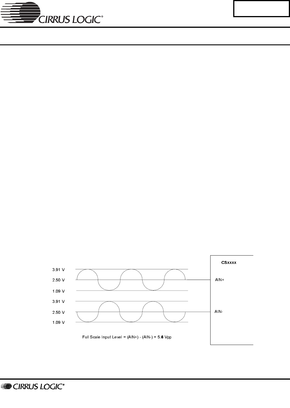
AN2412In the above example, the full scale input voltage is 5.64 Vpp (differentially), with each leg swinging2.82 Vpp. Please note that the full scale
AN2413where: R is the value of the resistor (in Ohms)C is the value of the capacitor (in Farads)In the input buffer shown in Figure 2, R = 10 kΩ and C
AN2414Figure 2 implements a common mode capacitor between the positive and negative nodes of the differen-tial inputs. This capacitor is commonly refe
AN2415Figure 3. Single-Ended to Differential Input Buffer3.4 Overview of the Filter Topology3.4.1 High Pass Filter and DC BiasingThe first stage of t
AN2416where: REQ is the value of the equivalent resistance (in Ohms)C is the value of the capacitor (in Farads)In the input buffer shown in Figure 3,
AN2417capacitors with a large voltage coefficient (such as general purpose ceramics) since they can degradesignal linearity.4. Single-Ended Input Buff
AN24184.4 Overview of Filter Topology #14.4.1 High Pass Filter and DC BiasingThe first stage of the buffer forms a high pass filter from the combinati
AN2419the input sampling rate of the converter. Also, low value resistors should be used to minimize the additionof resistor thermal noise.Figure 4 im
Related products and manuals for Hardware Cirrus-logic AN241
 (72 pages)
(4 pages)
(32 pages)
(63 pages)
(51 pages)
(36 pages)
(44 pages)
(59 pages)
(29 pages)
(91 pages)
(92 pages)
(91 pages)
(92 pages)
(57 pages)
(45 pages)
(30 pages)
(53 pages)
(50 pages)
(28 pages)
(53 pages)
(72 pages)
(4 pages)
(32 pages)
(63 pages)
(51 pages)
(36 pages)
(44 pages)
(59 pages)
(29 pages)
(91 pages)
(92 pages)
(91 pages)
(92 pages)
(57 pages)
(45 pages)
(30 pages)
(53 pages)
(50 pages)
(28 pages)
(53 pages)
© 2020, manymanuals.com. All rights reserved. | 1.421 s |
 Manymanuals.com
 Manymanuals.de
 Manymanuals.fr
 Manymanuals.it
 Manymanuals.pl
 Manymanuals.cz
 Manymanuals.es
 Manymanuals-pt.com
Comments to this Manuals