Cirrus-logic CS53L21 User Manual
Browse online or download User Manual for Hardware Cirrus-logic CS53L21. Cirrus Logic CS53L21 User Manual
- Page / 66
- Table of contents
- BOOKMARKS
- FEATURES 1
- SYSTEM FEATURES 1
- ™ Control) 1
- APPLICATIONS 2
- GENERAL DESCRIPTION 2
- TABLE OF CONTENTS 3
- LIST OF FIGURES 4
- LIST OF TABLES 5
- 6 DS700PP1 6
- 6
- Pin Name # Pin Description 6
- DS700PP1 7 7
- DS700PP1 9 9
- 10 DS700PP1 10
- ABSOLUTE MAXIMUM RATINGS 11
- SDOUT Code with HPF On 12
- Repeated 16
- = 100 μA) 18
- (Note 14) 18
- = -100 μA) 18
- POWER CONSUMPTION 19
- 4. APPLICATIONS 20
- 4.2 Hardware Mode 21
- Software 22
- Controls: 22
- 4.3.3 Digital Routing 23
- 4.3.4 Differential Inputs 23
- 24 DS700PP1 24
- 4.3.6 MIC & PGA Gain 25
- ADCx_ATT[7:0] and 26
- PGAx_VOL[4:0] volume 26
- ALCx is enabled 26
- 4.3.8 Noise Gate 27
- 4.4 Signal Processing Engine 28
- 4.4.1 Volume Controls 28
- 4.4.2 Mono Channel Mixer 28
- 4.5 Serial Port Clocking 29
- 4.5.1 Slave 30
- 4.5.2 Master 30
- 4.6 Digital Interface Formats 31
- 4.7 Initialization 32
- 4.10 Software Mode 34
- 4.10.1 SPI Control 34
- 4.10.2 I²C Control 34
- 4 5 6 7 24 25 35
- 4.10.3.1 Map Increment (INCR) 36
- 5. REGISTER QUICK REFERENCE 37
- 38 DS700PP1 38
- DS700PP1 39 39
- 6. REGISTER DESCRIPTION 40
- 76543210 41
- Reserved M/S 43
- 6.5 MIC Control (Address 05h) 44
- 6.6 ADC Control (Address 06h) 45
- AINx_MUX[1:0] 47
- PDN_PGAx 47
- 6.8 SPE Control (Address 09h) 48
- 7. ANALOG PERFORMANCE PLOTS 56
- 8.1 Auto Detect Enabled 57
- 8.2 Auto Detect Disabled 58
- 9. PCB LAYOUT CONSIDERATIONS 59
- 10.DIGITAL FILTERS 60
- 11.PARAMETER DEFINITIONS 61
- 12.PACKAGE DIMENSIONS 62
- THERMAL CHARACTERISTICS 62
- 13.ORDERING INFORMATION 63
- 14.REFERENCES 63
- 15.REVISION HISTORY 64
- DS700PP1 65 65
- 66 DS700PP1 66
Summary of Contents
Copyright © Cirrus Logic, Inc. 2006(All Rights Reserved)http://www.cirrus.comPreliminary Product InformationThis document contains information for a n
10 DS700PP1CS53L21+1.8V or +2.5VVQ0.1 µF1 µFDGNDVL0.1 µF+1.8V, 2.5 Vor +3.3VI²S/LJMCLKDIV2RESETLRCKAGNDMCLKSCLKVD* Capacitors must be C0G or equivalen
DS700PP1 11CS53L213. CHARACTERISTIC AND SPECIFICATION TABLES(All Min/Max characteristics and specifications are guaranteed over the Specified Operatin
12 DS700PP1CS53L21ANALOG CHARACTERISTICS (COMMERCIAL - CNZ)(Test Conditions (unless otherwise specified): Input sine wave (relative to digital full s
DS700PP1 13CS53L21ANALOG CHARACTERISTICS (AUTOMOTIVE - DNZ)(Test Conditions (unless otherwise specified): Input sine wave (relative to full scale): 1
14 DS700PP1CS53L21ADC DIGITAL FILTER CHARACTERISTICS 6. Response is clock-dependent and will scale with Fs. Note that the response plots (Figures 23
DS700PP1 15CS53L217. After powering up the CS53L21, RESET should be held low after the power supplies and clocks aresettled.8. See “Example System Clo
16 DS700PP1CS53L21SWITCHING SPECIFICATIONS - I²C CONTROL PORT(Inputs: Logic 0 = DGND, Logic 1 = VL, SDA CL=30pF)11. Data must be held for sufficient t
DS700PP1 17CS53L21SWITCHING CHARACTERISTICS - SPI CONTROL PORT(Inputs: Logic 0 = DGND, Logic 1 = VL)12. Data must be held for sufficient time to bridg
18 DS700PP1CS53L21DC ELECTRICAL CHARACTERISTICS (AGND = 0 V; all voltages with respect to ground.) 14. The DC current draw represents the allowed cur
DS700PP1 19CS53L21POWER CONSUMPTIONSee (Note 17)17. Unless otherwise noted, test conditions are as follows: All zeros input, slave mode, sample rate =
2 DS700PP1CS53L21APPLICATIONS Portable Audio Players Digital Microphones Digital Voice Recorders Voice Recognition Systems Audio/Video Capture Ca
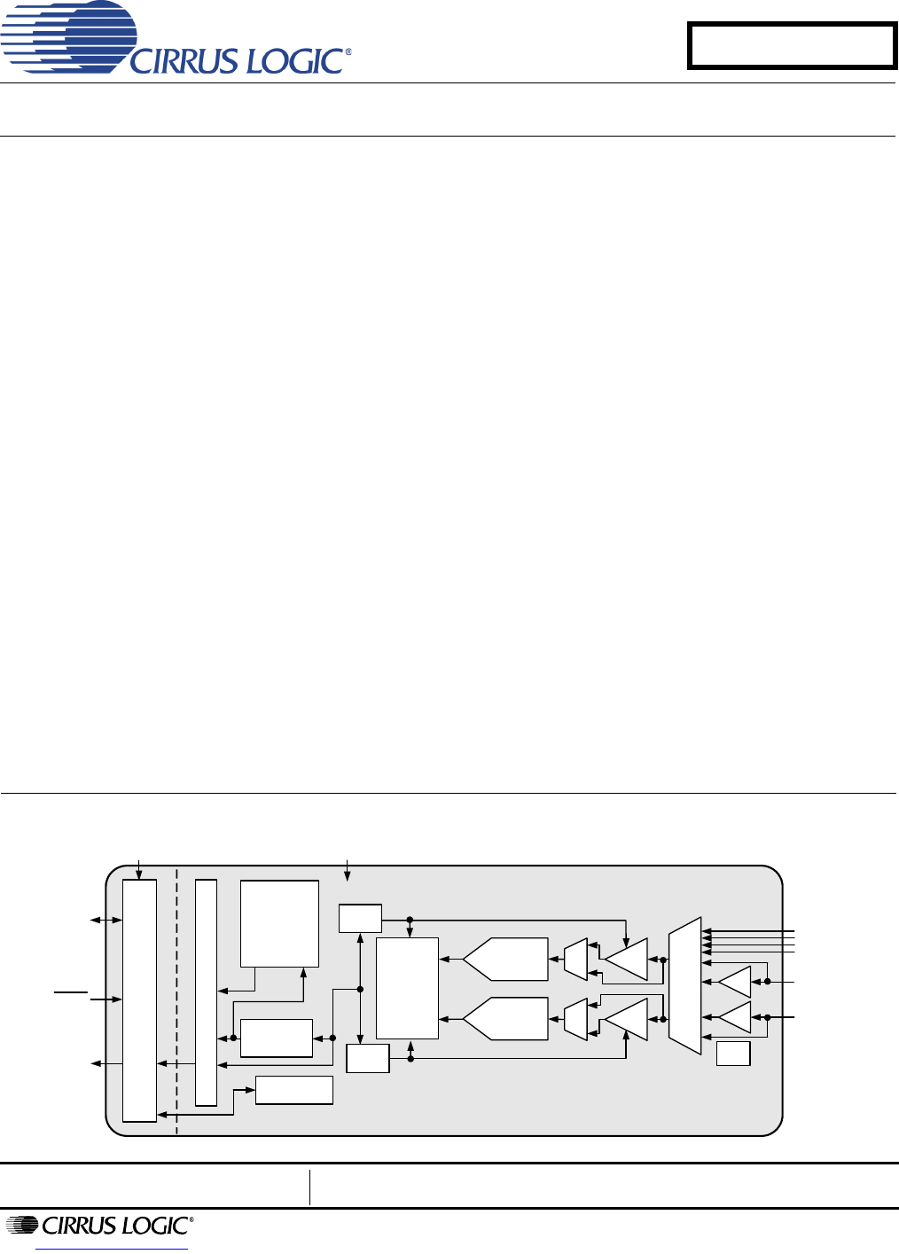
20 DS700PP1CS53L214. APPLICATIONS4.1 Overview4.1.1 ArchitectureThe CS53L21 is a highly integrated, low power, 24-bit audio A/D. The ADC operates at 64
DS700PP1 21CS53L214.2 Hardware Mode A limited feature-set is available when the A/D powers up in Hardware Mode (see “Recommended Power-Up Sequence” on
22 DS700PP1CS53L214.3 Analog InputsAINxA and AINxB are the analog inputs, internally biased to VQ, that accepts line-level and MIC-level sig-nals, al
DS700PP1 23CS53L214.3.2 High-Pass Filter and DC Offset Calibration The high-pass filter continuously subtracts a measure of the DC offset from the out
24 DS700PP1CS53L21The MICBIAS series resistor must be selected based on the requirements of the particular microphoneused. The MICBIAS output pin is s
DS700PP1 25CS53L214.3.5 Analog Input MultiplexerA stereo 4-to-1 analog input multiplexer selects between a line-level input source, or a mic-level inp
26 DS700PP1CS53L214.3.7 Automatic Level Control (ALC) When enabled, the ALC monitors the analog input signal after the digital attenuator, detects whe
DS700PP1 27CS53L214.3.8 Noise GateThe noise gate may be used to mute signal levels that fall below a programmable threshold. This preventsthe ALC from
28 DS700PP1CS53L214.4 Signal Processing EngineThe SPE provides various signal processing functions that apply to the ADC data. 4.4.1 Volume ControlsT
DS700PP1 29CS53L214.5 Serial Port ClockingThe A/D serial audio interface port operates either as a slave or master. It accepts externally generatedclo
DS700PP1 3CS53L21TABLE OF CONTENTS1. PIN DESCRIPTIONS - SOFTWARE (HARDWARE) MODE ... 61
30 DS700PP1CS53L214.5.1 SlaveLRCK and SCLK are inputs in Slave Mode. The speed of the A/D is automatically determined based onthe input MCLK/LRCK rati
DS700PP1 31CS53L214.5.3 High-Impedance Digital OutputThe serial port may be placed on a clock/data bus that allows multiple masters for the serial por
32 DS700PP1CS53L21 4.7 InitializationThe initialization and Power-Down sequence flowchart is shown in Figure 17 on page 33. The A/D enters aPower-Down
DS700PP1 33CS53L214.9 Recommended Power-Down SequenceTo minimize audible pops when turning off or placing the A/D in standby,1. Mute the ADC’s. 2. Set
34 DS700PP1CS53L214.10 Software ModeThe control port is used to access the registers allowing the A/D to be configured for the desired operationalmode
DS700PP1 35CS53L21increment bit in MAP allows successive reads or writes of consecutive registers. Each byte is separatedby an acknowledge bit. The AC
36 DS700PP1CS53L214.10.3 Memory Address Pointer (MAP) The MAP byte comes after the address byte and selects the register to be read or written. Refer
DS700PP1 37CS53L215. REGISTER QUICK REFERENCE Software mode register defaults are as shown. “Reserved” registers must maintain their default state.Add
38 DS700PP1CS53L21p50default0 00000000Eh Vol. Control ADCMIXAMUTE_ADCMIXAADCMIXAVOL6ADCMIXA VOL5ADCMIXA VOL4ADCMIXA VOL3ADCMIXA VOL2ADCMIXA VOL1ADCMIX
DS700PP1 39CS53L211Dh ALC Release RateReserved Reserved ALC_RRATE5ALC_RRATE4ALC_RRATE3ALC_RRATE2ALC_RRATE1ALC_RRATE0p52default0 01111111Eh ALC Thresh-
4 DS700PP1CS53L216.1 Chip I.D. and Revision Register (Address 01h) (Read Only) ... 406.2 Power
40 DS700PP1CS53L216. REGISTER DESCRIPTIONAll registers are read/write except for the chip I.D. and Revision Register and Interrupt Status Register whi
DS700PP1 41CS53L21Power Down PGA X (PDN_PGAX)Default: 00 - Disable1 - EnableFunction:PGA channel x will either enter a power-down or muted state when
42 DS700PP1CS53L21Speed Mode (SPEED[1:0])Default: 0111 - Quarter-Speed Mode (QSM) - 4 to 12.5 kHz sample rates10 - Half-Speed Mode (HSM) - 12.5 to 25
DS700PP1 43CS53L216.4 Interface Control (Address 04h)Master/Slave Mode (M/S)Default: 00 - Slave1 - MasterFunction:Selects either master or slave opera
44 DS700PP1CS53L21ADC I²S or Left-Justified (ADC_I²S/LJ)Default: 00 - Left-Justified1 - I²SFunction:Selects either the I²S or Left-Justified digital i
DS700PP1 45CS53L21ADCx 20 dB Digital Boost (ADCx_DBOOST)Default: 00 - Disabled1 - EnabledFunction:Applies a 20 dB digital gain to the input signal on
46 DS700PP1CS53L21ADCX High-Pass Filter Freeze (ADCX_HPFRZ)Default: 00 - Continuous DC Subtraction1 - Frozen DC SubtractionFunction:The high-pass filt
DS700PP1 47CS53L216.7 ADCx Input Select, Invert & Mute (Address 07h)ADCX Input Select Bits (AINX_MUX[1:0])Default: 00 Function:Selects the specifi
48 DS700PP1CS53L216.8 SPE Control (Address 09h)SPE_ENABLEDefault: 00 - Reserved1 - ADC Serial Port to SPEFunction:Selects the digital signal source fo
DS700PP1 49CS53L21SPE Soft Ramp and Zero Cross Control (SPE_SZC[1:0]) Default = 1000 - Immediate Change01 - Zero Cross 10 - Soft Ramp11 - Soft Ramp on
DS700PP1 5CS53L21Figure 21.AIN & PGA Selection ...
50 DS700PP1CS53L21ALCX Zero Cross Disable (ALCX_ZCDIS)Default: 00 - Off1 - OnFunction:Overrides the ZCROSSx bit setting for the ADC. When this bit is
DS700PP1 51CS53L21Function:The level of ADCX can be adjusted in 1.0 dB increments as dictated by the ADCx Soft and Zero Cross bits(SOFTx & ZCROSSx
52 DS700PP1CS53L21Function:Implements mono mixes of the left and right channels as well as a left/right channel swap. 6.13 ALC Enable & Attack Rat
DS700PP1 53CS53L21Function:Sets the rate at which the ALC releases the PGA & digital attenuation from levels below the minimum settingin the ALC t
54 DS700PP1CS53L216.16 Noise Gate Configuration & Misc. (Address 1Fh)Noise Gate Channel Gang (NG_ALL)Default: 00 - Disabled1 - EnabledFunction:Gan
DS700PP1 55CS53L216.17 Status (Address 20h) (Read Only)For all bits in this register, a “1” means the associated error condition has occurred at least
56 DS700PP1CS53L217. ANALOG PERFORMANCE PLOTS7.1 ADC_FILT+ Capacitor Effects on THD+NThe value of the capacitor on the ADC_FILT+ pin, 16, affects the
DS700PP1 57CS53L218. EXAMPLE SYSTEM CLOCK FREQUENCIES 8.1 Auto Detect Enabled*The”MCLKDIV2” pin 4 must be set HI.Sample RateLRCK (kHz)MCLK (MHz)1024x
58 DS700PP1CS53L218.2 Auto Detect Disabled Sample RateLRCK (kHz)MCLK (MHz)512x 768x 1024x 1536x 2048x 3072x8 - 6.1440 8.1920 12.2880 16.3840 24.576011
DS700PP1 59CS53L219. PCB LAYOUT CONSIDERATIONS9.1 Power Supply, GroundingAs with any high-resolution converter, the CS53L21 requires careful attention
6 DS700PP1CS53L211. PIN DESCRIPTIONS - SOFTWARE (HARDWARE) MODE Pin Name # Pin DescriptionLRCK1Left Right Clock (Input/Output) - Determines
60 DS700PP1CS53L2110.DIGITAL FILTERSFigure 23. ADC Passband Ripple Figure 24. ADC Stopband RejectionFigure 25. ADC Transition Band Figure 26. ADC
DS700PP1 61CS53L2111.PARAMETER DEFINITIONSDynamic RangeThe ratio of the rms value of the signal to the rms sum of all other spectral components over t
62 DS700PP1CS53L2112.PACKAGE DIMENSIONS 1. Dimensioning and tolerance per ASME Y 14.5M-1995.2. Dimensioning lead width applies to the plated termi
DS700PP1 63CS53L2113.ORDERING INFORMATION 14.REFERENCES1. Cirrus Logic, AN18: Layout and Design Rules for Data Converters and Other Mixed Signal Devic
64 DS700PP1CS53L2115.REVISION HISTORY Revision ChangesA1Initial ReleasePP1Adjusted the minimum voltage specification in “Specified Operating Condition
DS700PP1 65CS53L21Contacting Cirrus Logic SupportFor all product questions and inquiries, contact a Cirrus Logic Sales Representative. To find the one
66 DS700PP1CS53L21
DS700PP1 7CS53L21TSTO9Test Out (Output) - This pin is an output used for test purposes only and must be left “floating” (no con-nection external to th
8 DS700PP1CS53L211.1 Digital I/O Pin CharacteristicsThe logic level for each input should not exceed the maximum ratings for the VL power supply. Pin
DS700PP1 9CS53L212. TYPICAL CONNECTION DIAGRAMSFigure 1. Typical Connection Diagram (Software Mode)1 µF+1.8 V or +2.5 VVQ0.1 µF1 µFDGNDVL0.1 µF+1.8 V
Related products and manuals for Hardware Cirrus-logic CS53L21
 (33 pages)
(67 pages)
(14 pages)
(37 pages)
(24 pages)
(54 pages)
(4 pages)
(4 pages)
(2 pages)
(4 pages)
(44 pages)
(38 pages)
(16 pages)
(36 pages)
(3 pages)
(2 pages)
(46 pages)
(20 pages)
(38 pages)
(46 pages)
(33 pages)
(67 pages)
(14 pages)
(37 pages)
(24 pages)
(54 pages)
(4 pages)
(4 pages)
(2 pages)
(4 pages)
(44 pages)
(38 pages)
(16 pages)
(36 pages)
(3 pages)
(2 pages)
(46 pages)
(20 pages)
(38 pages)
(46 pages)
© 2020, manymanuals.com. All rights reserved. | 3.975 s |
 Manymanuals.com
 Manymanuals.de
 Manymanuals.fr
 Manymanuals.it
 Manymanuals.pl
 Manymanuals.cz
 Manymanuals.es
 Manymanuals-pt.com
Comments to this Manuals