Cirrus-logic CDB5345 User Manual
Browse online or download User Manual for Hardware Cirrus-logic CDB5345. Cirrus Logic CDB5345 User Manual
- Page / 27
- Table of contents
- BOOKMARKS
- Evaluation Board for CS5345 1
- TABLE OF CONTENTS 2
- LIST OF FIGURES 3
- LIST OF TABLES 3
- 1. SYSTEM OVERVIEW 4
- 1.7 External Control Headers 5
- 1.8 Analog Inputs 5
- 1.9 Analog Outputs 5
- 1.10 Serial Control Port 5
- 1.11 USB Control Port 5
- 2.1 Clock Routing 6
- 2.2 Data Routing 6
- 3.1 CDB5345 Controls Tab 7
- 3.2 Register Maps Tab 8
- 10 DS658DB1 10
- Addr Function 7 6 5432 1 0 10
- 5. FPGA REGISTER DESCRIPTION 11
- DS658DB1 15 15
- 8. CDB SCHEMATICS 16
- DS658DB1 17 17
- 18 DS658DB1 18
- DS658DB1 19 19
- 20 DS658DB1 20
- DS658DB1 21 21
- 22 DS658DB1 22
- DS658DB1 23 23
- 9. CDB LAYOUT 24
- DS658DB1 25 25
- 26 DS658DB1 26
- 10.REVISION HISTORY 27
Summary of Contents
Copyright © Cirrus Logic, Inc. 2005(All Rights Reserved)Cirrus Logic, Inc.www.cirrus.comCDB5345Evaluation Board for CS5345Featuresz Single-ended Analo
CDB534510 DS658DB14. FPGA REGISTER QUICK REFERENCEThis table shows the register names and their associated default values.Addr Function 7 6 5432 1 001
CDB5345DS658DB1 115. FPGA REGISTER DESCRIPTION5.1 CODE REVISION ID - ADDRESS 01HFunction:Identifies the revision of the FPGA code. This register is Re
CDB534512 DS658DB15.3 SUBCLOCK SOURCE CONTROL - ADDRESS 03H5.3.1 SUBCLOCK SOURCE (BITS 1:0)Default = 01Function:This bit selects the source of the CS5
CDB5345DS658DB1 136. CDB CONNECTORS, JUMPERS, AND SWITCHES CONNECTORReference Designator INPUT/OUTPUT SIGNAL PRESENT+5V J1 Input+5.0 V Power Supp
CDB534514 DS658DB1 JUMPER PURPOSE POSITION FUNCTION SELECTEDJ3 Selects the source of voltage for the VLC supply.+1.8 V+2.5 V+3.3 V+5 V*Voltage source
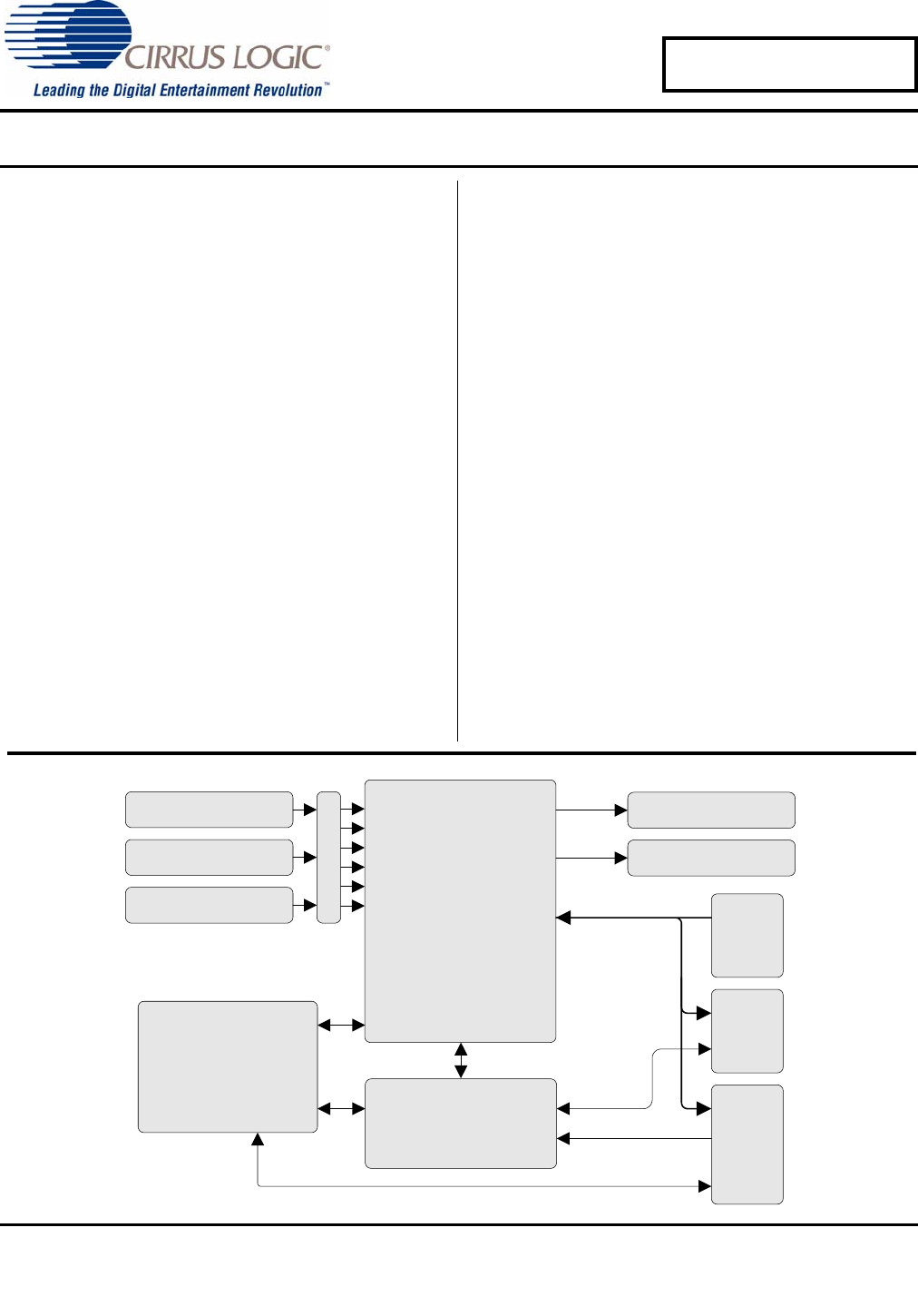
CDB5345DS658DB1 157. CDB BLOCK DIAGRAM CS5345FPGACS8406Passive Input FilterActive Input FilterHeaderMicrophone InputActive Output FilterCann
CDB534516 DS658DB18. CDB SCHEMATICS Figure 4. CS5345
CDB5345DS658DB1 17 Figure 5. Analog Inputs
CDB534518 DS658DB1 Figure 6. Analog Outputs
CDB5345DS658DB1 19 Figure 7. S/PDIF Output
CDB53452 DS658DB1TABLE OF CONTENTS1. SYSTEM OVERVIEW ...
CDB534520 DS658DB1 Figure 8. Control Port
CDB5345DS658DB1 21 Figure 9. FPGA
CDB534522 DS658DB1 Figure 10. Discrete Clock Routing and Level Shifting
CDB5345DS658DB1 23 Figure 11. Power
CDB534524 DS658DB19. CDB LAYOUT Figure 12. Silk Screen
CDB5345DS658DB1 25 Figure 13. Topside Layer
CDB534526 DS658DB1 Figure 14. Bottom side Layer
CDB5345DS658DB1 2710.REVISION HISTORY Revision Date ChangesDB1 February 2005 Initial ReleaseTable 6. Revision HistoryContacting Cirrus Logic SupportFo
CDB5345DS658DB1 3LIST OF FIGURESFigure 1. CDB5345 Controls Tab...
CDB53454 DS658DB11. SYSTEM OVERVIEW The CDB5345 evaluation board is an excellent means for evaluating the CS5345 ADC. Analog and digital audio sig-nal
CDB5345DS658DB1 5The oscillator is mounted in pin sockets, allowing easy removal or replacement. The board is shipped witha 12.2880 MHz crystal oscill
CDB53456 DS658DB12. SYSTEM CLOCKS AND DATAThe CDB5345 implements comprehensive clock routing capabilities. Configuration of the clock routing can be e
CDB5345DS658DB1 73. PC SOFTWARE CONTROLThe CDB5345 is shipped with a Microsoft Windows® based graphical user interface which allows control over theCS
CDB53458 DS658DB13.2 Register Maps TabThe Register Maps tab provides low level control over the register level settings of the CS5345, CS8406,and FPGA
CDB5345DS658DB1 93.3.2 Oscillator Clock - ADC Ch 2 In to In to SPDIF OutUsing the pre-configured script file named “Oscillator Clock - ADC Ch 2 In to
Related products and manuals for Hardware Cirrus-logic CDB5345
 (23 pages)
(16 pages)
(7 pages)
(4 pages)
(23 pages)
(16 pages)
(42 pages)
(42 pages)
(42 pages)
(24 pages)
(24 pages)
(38 pages)
(24 pages)
(22 pages)
(32 pages)
(40 pages)
(44 pages)
(24 pages)
(8 pages)
(4 pages)
(23 pages)
(16 pages)
(7 pages)
(4 pages)
(23 pages)
(16 pages)
(42 pages)
(42 pages)
(42 pages)
(24 pages)
(24 pages)
(38 pages)
(24 pages)
(22 pages)
(32 pages)
(40 pages)
(44 pages)
(24 pages)
(8 pages)
(4 pages)
© 2020, manymanuals.com. All rights reserved. | 0.670 s |
 Manymanuals.com
 Manymanuals.de
 Manymanuals.fr
 Manymanuals.it
 Manymanuals.pl
 Manymanuals.cz
 Manymanuals.es
 Manymanuals-pt.com
Comments to this Manuals